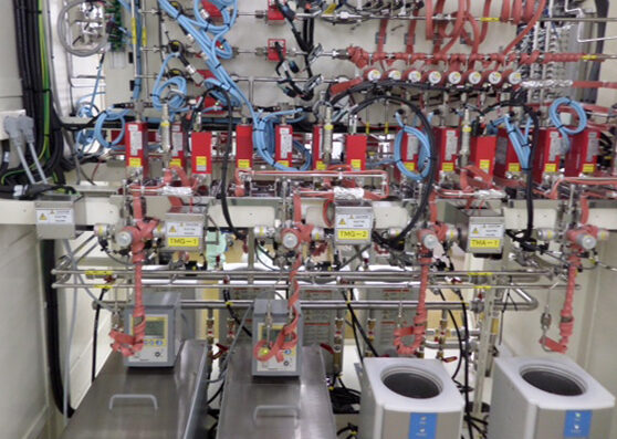
EEA served as the prime consultant and MEP engineer to lead a modernization program for a critical aging semiconductor fab. The program involved approximately 100 individual projects to replace obsolete tools, expand and modify cleanroom manufacturing space, and upgrade utility systems – all while maintaining operations in a highly congested environment. All tool installs were first of kind for the facility, with many requiring creative solutions to modify spaces due to the increased footprint and height of the new tools. Utility systems upgraded included corrosive exhaust, process cooling water, UPS, UPW, building automation, and CO2 fire suppression. Laser scanning was performed to generate more accurate as-built conditions as existing documentation was outdated.
Cross discipline coordination was critical to this project, especially given space constraints in the fab. In addition to traditional MEP design services, EEA managed a consultant team including process engineers, architects, structural engineers, and fire protection engineers. One of the unique challenges was planning the sequence of project execution given the complex nature of removing and installing tools and upgrading utility systems in a working fab. We integrated ourselves closely with the customer to develop a workable plan, which included the needs of process owners, facility system owners, and management.
Flexibility and Focus
As the project progressed, the tool set requirements for the customer evolved. In addition, down time constraints and production needs drove changes to design packages that had to be incorporated in a timely manner. EEA maintained both flexibility and focus to meet the customer’s needs.