High Tech / Semiconductor

Semiconductor Fab Design

When choosing a design firm, you want a partner who has first-hand experience working in the semiconductor industry. EEA provides design for cleanrooms, tool installations, and utility systems for semiconductor fabs and electronics manufacturing facilities.

Our experience covers a range of utility systems:

  • Compressed Air
  • DI/UPW Systems
  • Chemical Delivery Systems
  • Wastewater
  • Bulk/Specialty Gases
  • HPM Monitoring
  • Process Cooling Water
  • Process Vacuum
  • Corrosive/VOC exhaust

Our tool installation experience includes:

  • Photolithography
  • SEM
  • Wet Bench
  • MOCVD
  • Diffusion
  • Ion Implant
  • MBE
  • Metrology
  • CMP
  • PVD/CVD
  • Dry Etch
  • ALE/ALD
  • Plating
  • EPI
  • BCD/CDU

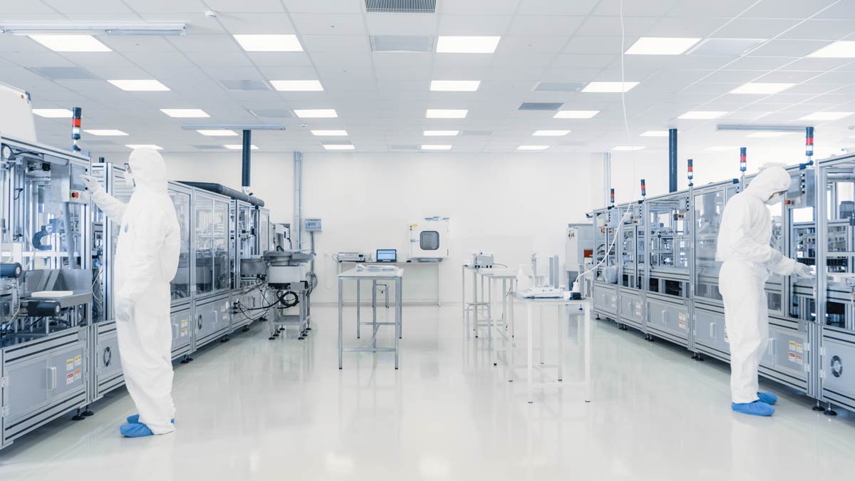
Custom Solutions to Custom Problems

We understand that each project and client has unique needs and priorities. Our experience across numerous facilities allows us to customize solutions and deliver high quality designs to address challenging problems.

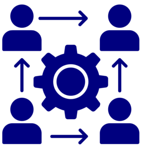
Managing the Entire Process

Our goal is to be your long-term, one-stop shop for managing projects. We maintain excellent relationships with specialty process designers, structural engineers, and architects with extensive experience in semiconductor fabs and the hi-tech industry. We bring those relationships to the table as needed for each client, managing both the project and the people involved.

We are known for our responsiveness and welcome an open line of communication with our partners. Let us know how we can partner with you.

Related