High Tech / Semiconductor

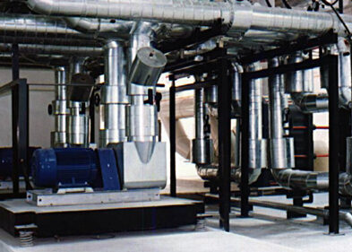
Singapore Electronics Manufacturing Plant

A Record Breaking Facility In 1999 EEA completed work on a new 3-story, 550,000 square foot electronic products manufacturing facility in Singapore.  The project team delivered the facility, including the first production line, in 13 months. This set the Singapore fast track construction record at that time. Unique Role EEA wore a variety of hats
Read More »

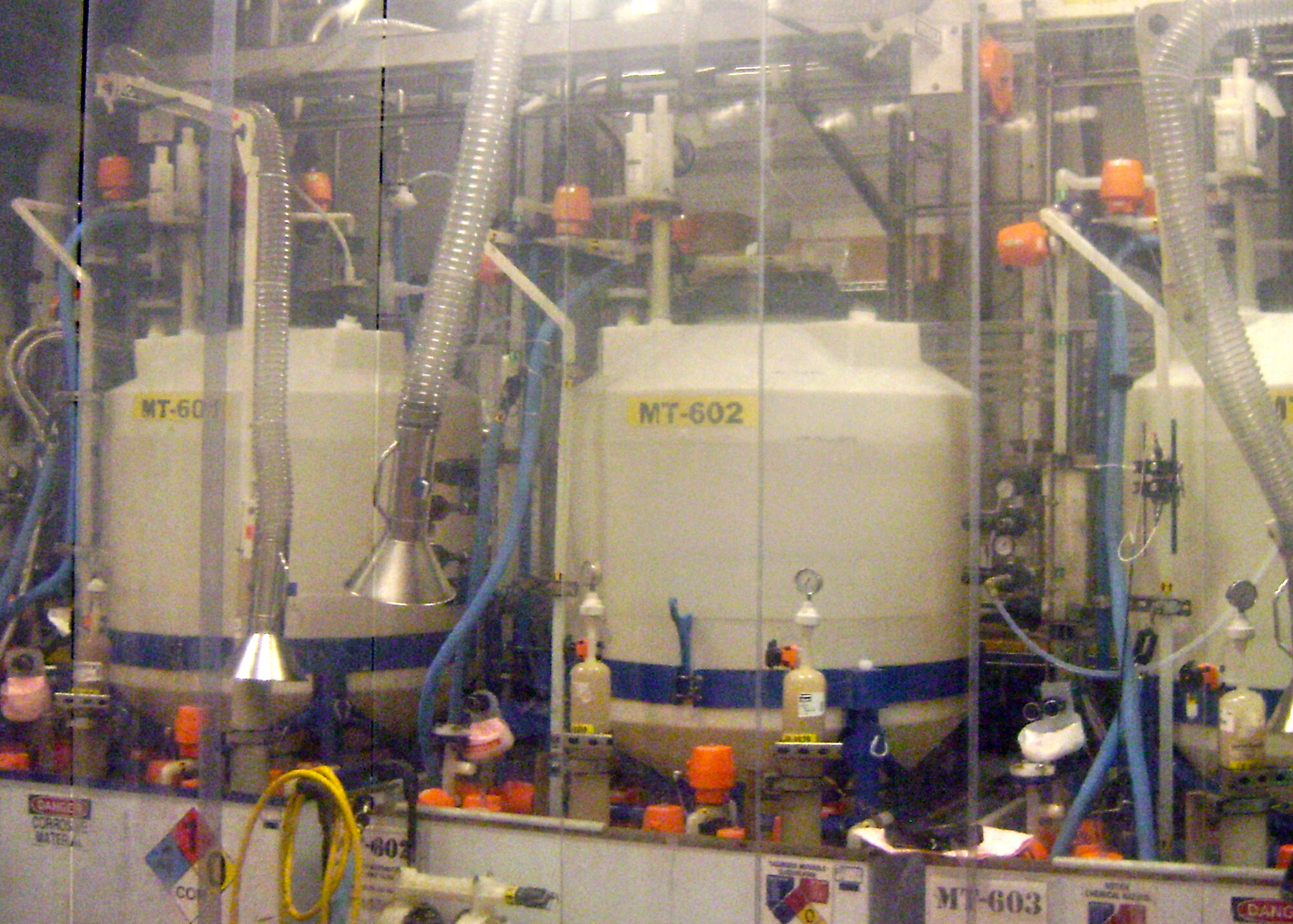
Chemical Packaging Line Expansion

Volatile Situation In 2013 a high-purity chemical supplier to the semiconductor industry wanted to expand their mixing and packaging area. Due to the flammability of the process materials, the expansion mixing area was designated electrical Class 1 Division 2.  The existing Class 10,000 clean packaging area was also modified and separated into smaller rooms using

Read More »

Semiconductor Fab Modernization

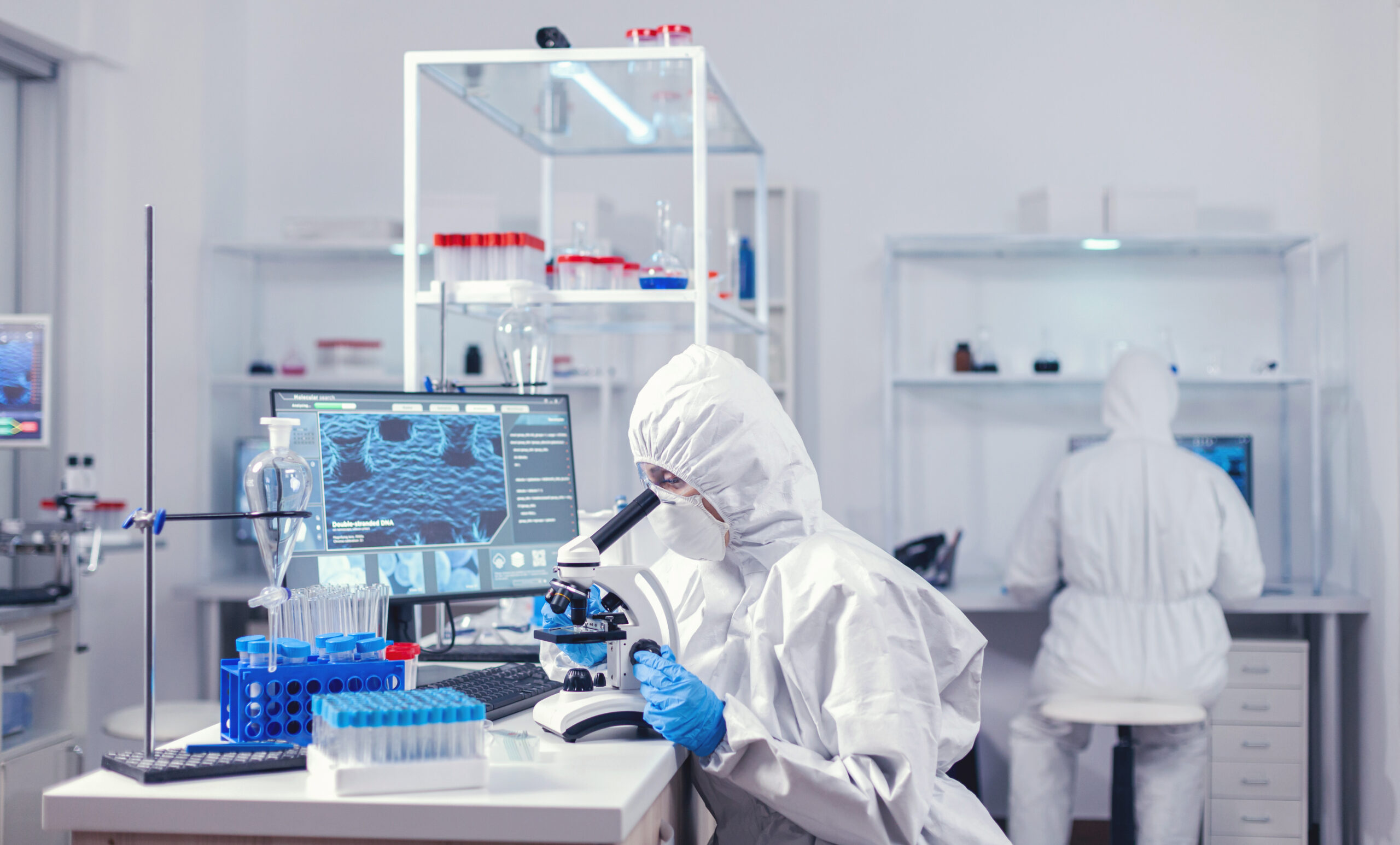
EEA served as the prime consultant and MEP engineer to lead a modernization program for a critical aging semiconductor fab.  The program involved approximately 100 individual projects to replace obsolete tools, expand and modify cleanroom manufacturing space, and upgrade utility systems – all while maintaining operations in a highly congested environment.  All tool installs were

Read More »

Pickle Research Center – MER Clean Room

Where to Build a Clean Room? Researchers at the University of Texas J.J. Pickle Research Center needed more clean room space in the Microelectronics Research building, but had occupied all of the available clean space in the building. The College of Engineering needed to locate the new 4,000 square foot clean room adjacent to existing

Read More »